Screen printed diffusions and contacts for ultra-thin silicon wafers
In collaboration with Ferro Electronic Materials the University of the Basque Country has developed a new manufacturing process able to be used with ultra-thin silicon wafers, proven on 70 µm thick wafers. This process conducts to bifacial structures with over 90% of bifaciality.
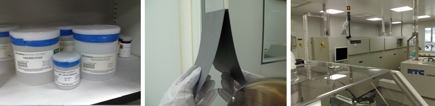
The process includes new boron screen printed diffusions [1] and new silver pastes to contact these boron emitters [2].
- [1] F. Recart, I. Freire, L. Pérez, R. Lago-Aurrekoetxea, J.C. Jimeno, G. Bueno. Screen printed boron emitters for solar cells. Solar Energy Materials & Solar Cells 91 (2007) 897–902
- [2] R. Lago, L. Pérez, H. Kerp, I. Freire, I. Hoces, N. Azkona, F. Recart and J.C. Jimeno, Screen printing metallization of boron emitters. Prog. Photovolt: Res. Appl. 2010; 18:20–27
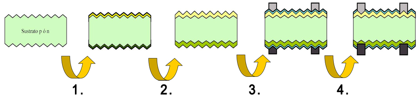
p - n substrate:
- Screen-printing of phosphorus and boron pastes
- Simultaneous diffusion in IR furnace
- Screen-printing of metallic pastes
- Firing of metallic pastes in IR furnace

Ferro Electronic Material Systems
Frontstraat 2, 5405 PB Uden, The Netherlands
- e-mail: kerpH@ferro.com
- Phone: +31.413.283372